Chip-scale package (CSP): the MEMS and IC chips are attached via
Price: $ 92.00
4.5(601)
Download scientific diagram | Chip-scale package (CSP): the MEMS and IC chips are attached via face-to-face flip-chip bonding. (b) Photograph of a 3-axis accelerometer (VTI, CMA 3000) fabricated using chip-on-MEMS technology. Package dimensions: 2 × 2 × 1 mm3. From Ref 61. from publication: Integrating MEMS and ICs | The majority of microelectromechanical system (MEMS) devices must be combined with integrated circuits (ICs) for operation in larger electronic systems. While MEMS transducers sense or control physical, optical or chemical quantities, ICs typically provide functionalities | Micro-Electrical-Mechanical Systems, Transducers and Devices | ResearchGate, the professional network for scientists.
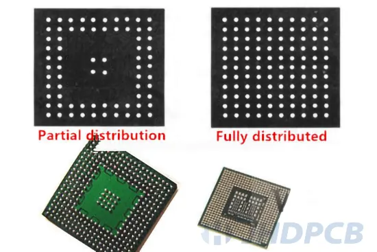
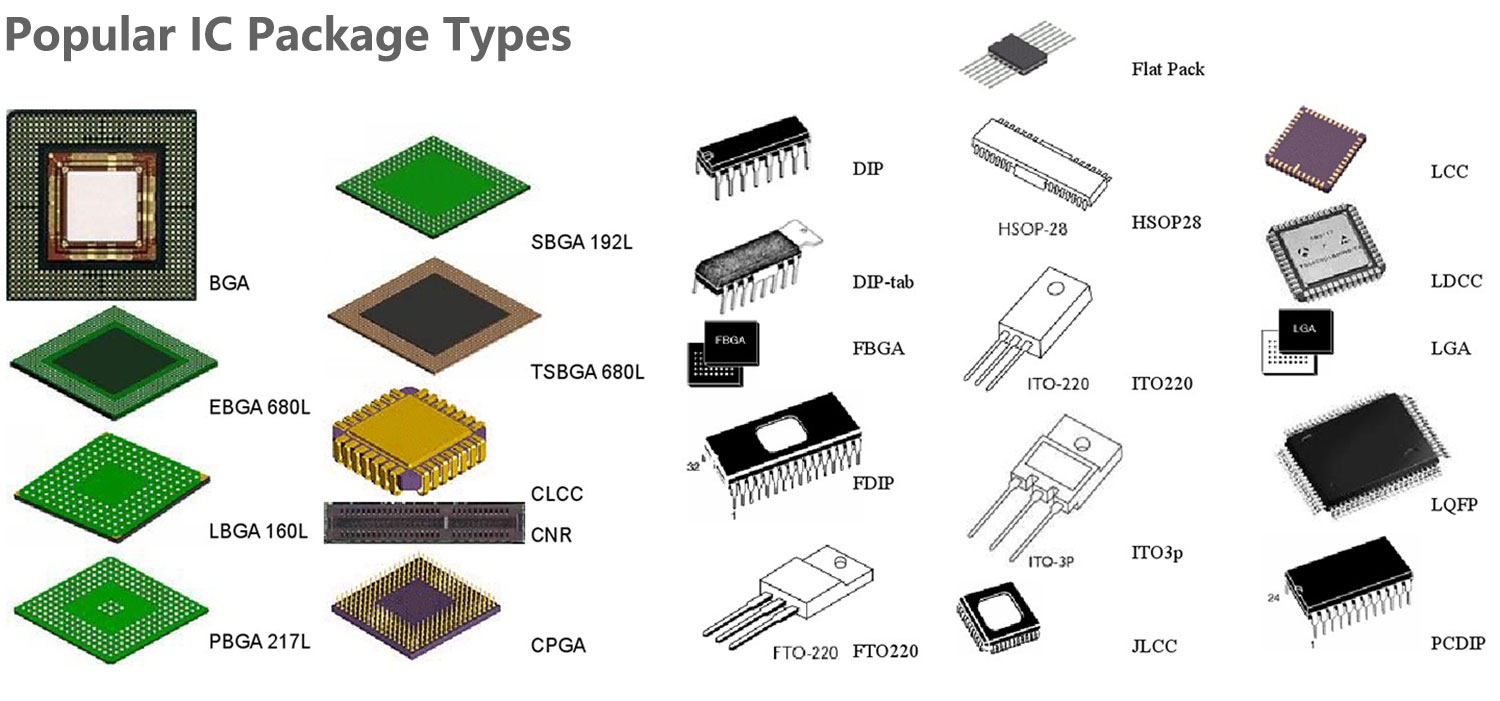
Chip Scale Package: A Guide To CSP Package Forms And Types - Jhdpcb
IC Substrate - Basic Introduction to Integrated Chip Substrate - NextPCB
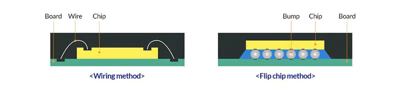
Flip Chip CSP, Advanced Packaging

Chip Scale Packages - an overview

The 3D MEMS Scale Packaging Concept: a stack of four chips.
industry news - Chip Scale Review

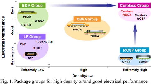
The Next Advanced Packages
IC Package Types and Their Features - Ovaga Technologies
IC Substrate - Basic Introduction to Integrated Chip Substrate - NextPCB
Chip Scale Package: A Guide To CSP Package Forms And Types - Jhdpcb

Illustration of a µBGA-W compliant CSP package in which a compliant die

Figure 3 from Advancements in Stacked Chip Scale Packaging (S-CSP), Provides System-in-a-Package Functionality for Wireless and Handheld Applications White Paper

Dual-Inline Package - an overview